
KINTEC Company aims at
supplying high quality indium-tin-oxide ITO glass, ITO PET film, ITO PEN film,
FTO glass and other TCO substrates at a low price, which is particularly
suitable for the academic and research purposes. More importantly, we provide ITO patterning service from small to large
ITO glasses and plastic films, and fast
international delivery service. We are also capable of volume production.
In R&D, our professional
team in

Our high quality ITO glass and wafer can be
employed as transparent conducting substrates for the applications of:
- Small-molecule Organic light-emitting diodes (OLED), (our sample
devices)
- Polymer light-emitting diodes (PLEDs),
- Organic photovoltaic diodes (PVs),
- Organic transistors (OTFTs),
- Biosensors,
- Electroluminescence
devices,
- Chip-on-glass (COG) and liquid crystal displays (LCD) (e.g. TN,
STN)
- ITO touch panels for LCDs, PDAs, cellphones, etc.
- Transparent EMF/EMI/EMC/RFI/HF shielding, scanner windows
- Flat antennas for mobile communication
- Heatable slides and cover slips
We
examine the ITO quality and test the corresponding performance in OLED/PLED
devices.
Due to
demand of advanced
materials for next generation electronic applications, we supply
various high quality materials, including sublimed organic
electronic materials for the research of organic light-emitting diodes (OLED
materials), solar cells, and transistors. Under standard device testing
scheme, our EL materials are verified in terms of electroluminescence
performance. For available OLED, OPV, OTFT materials, please contact sales@kintec.hk.
NEWS
Jan 2012
- JDA signed with
expert in
Sept 2010
- Shanghai Office
set up
Feb 2009
Recently, we extend our business to:
- LCD panels (TN, STN prototypes for display
applications)
- Substrate / wafer carriers (Remark: 1.5” carrier for
25mm x 25mm samples)
- Fluorine-Tin-Oxide substrates (FTO)
- UV grade fused silica, single crystal quartz substrates
(Double side polished)
- Silicon wafers (polished Prime/ EPI / reclaim /
test)
- Inorganic particles (Si, ZnO, Au, Ag)
|
Main Products |
|
|
1. Substrates |
ITO coated glass |
|
|
ITO coated plastic film (PET, PEN, etc) |
|
|
Fluorine-tin-oxide FTO coated glass |
|
|
UV grade fused silica |
|
|
Single crystal quartz |
|
|
Silicon wafers (Prime /Test / Reclaim) |
|
2. Advanced Electronic Materials |
Sublimed Organic small molecules High purity Organic polymer (suitable for OLEDs, OPVs, OTFTs) |
|
|
Silicon, ZnO, Au, Ag, etc powders /
nano-particles |
|
|
Zinc oxide particles |
|
3. LCD prototypes |
TN LCD panels STN LCD panels |
|
4. Touch panels |
4-wire, 5-wire, capacitive touch panels |
|
5. Sample containers |
1.5” sample carriers (good for a 25mm x 25mm slide) 1”, 2”, 3”, 4” traditional wafer carriers (anti-static carriers available) |
|
6. Cleaning |
FPD and ITO glass detergents |
Product
Details
Indium-tin-oxide (ITO) coated substrates
- Bare (unpatterned)
indium-tin-oxide (ITO) glass
(e.g. 15 ohm/sq.; 25 mm x 25 mm; < USD 1.5)
- Patterned indium-tin-oxide (ITO) glass
(e.g. 15 ohm/sq.; 25 mm x 25 mm; <
USD 1.5)
- Bare ITO coated plastic film [PET, PEN]
- Patterned ITO coated plastic films [PET, PEN]
Discount 60 ohm/sq ITO coated
PET film (0.125mm)
USD 15/pc
(200mm x 5m) (min order 10 pcs)
USD 75/m2 (200mm x 100m)
|
ITO glass |
|
|
Specifications |
|
|
Product configuration |
Glass / SiO2
buffer (~23 nm) / ITO |
|
ITO coating |
Magnetron sputtering |
|
ITO patterning |
Photolithography |
|
Size |
Any size up to 14”x 16” |
|
Typical sheet resistance (ohm/sq) |
6, 10, 13, 15, 20, 60, 100,
250, etc (Others are also available
for volume production) |
|
Substrate thickness (mm) |
0.4, 0.55, 0.7, and 1.1 |
|
Pre-patterned |
Via photofilm
or Cr mask |
|
ITO plastic film |
|
|
Specifications |
|
|
Product configuration |
Polyethylene terephthalate (PET) / ITO PEN / ITO |
|
ITO coating |
Magnetron sputtering |
|
ITO patterning |
Lithography / Screen-printing
/ Laser patterning |
|
Size |
Sheet / roll (width <=1200
mm) |
|
Typical sheet resistance (ohm/sq) |
6, 10, 14, 20, 50, 60, 80,
100, 120, 150, 250, 300, 350, 450,
500 |
|
Substrate thickness (mm) |
0.125, 0.175, 0.188, 0.21 |
|
ITO Physical properties |
|
|
ITO Work function |
4.9 eV (UPS) We offer consultation for ITO cleaning |
|
4.8-4.9 eV (UPS) (after exposed to Chloro-based
solvents) |
|
|
ITO thickness |
Usually, up to 125 nm |
|
Micro-roughness |
RMS 1-2
nm (Digital Instrument 3100 AFM) |
|
Optical transmission |
> 85% at 555 nm. |
Fluorine-tin-oxide (FTO) coated substrates
- For solar/photovoltaics
applications: e.g dye-sensitized cells, organic solar cells
- For display
applications: transparnt conducting electrode for top emitting displays
- Others: heated glass,
mirrors, computer screens, EMI/RFI shielding, oven windows, electro-optical,
insulating applications
- Bare and Patterned fluorine-tin-oxide (FTO) glass
- FTO products: Pilkington FTO glass (TEC Glass), Nippon Sheet Glass FTO glass,
|
Pilkington FTO glass (TEC series) for solar applications |
||
|
Specifications |
||
|
FTO glass manufacturer |
|
|
|
Size |
Up to 14”x 16” (355mm x
406mm) |
|
|
Typical sheet resistance (ohm/sq) |
TEC# |
ohm/sq |
|
8 15 70 250 1000 1000 |
<= 9 <= 14 <= 80 <= 280 <= 3000 <= 5000 |
|
|
Substrate |
Clear soda lime float glass ASMT C-1036-91 or better |
|
|
Substrate thickness (mm) |
2.5 - 6 |
|
|
Optical transmission |
Daylight: 83-88 % Solar: 61-81 % |
|
|
Haze |
TEC# |
% |
|
8 15 70, 250, 1000 |
> 2 < 0.7 < 0.5 |
|
|
Product features |
Color neutral, low emissivity Durable pyrolytic
(hard coat) surface Bendable |
|
|
for solar applications |
|
|
Specifications |
|
|
FTO glass manufacturer |
Nippon Sheet Glass Co. Ltd., |
|
Size |
<= 14” x 16” or 300mm x 300mm |
|
Typical sheet resistance (ohm/sq) |
< 7 and 13 |
|
Substrate |
Soda lime float glass |
|
Substrate thickness (mm) |
2.2 and 3.1 +/- 0.2 |
|
Visible transmission |
> 77 % |
|
Haze |
>8 % |
|
Normal FTO glass |
|
|
Specifications |
|
|
FTO glass manufacturing |
PRC |
|
Size |
Any size up to 300mm x 300mm |
|
Typical sheet resistance (ohm/sq) |
<15 |
|
Substrate |
Clear soda lime float glass |
|
Substrate thickness |
2.2 mm |
Remark: Customer services including
patterning are available. We can offer patterning service for your ITO
substrates.
Sample / wafer carriers
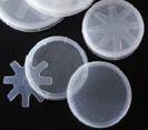
- Sample facing-down avoids any contact
with sample surface
- Retaining sample by spring minimizes particle
generation
- Lock-stacking by convenient screws: cover-on-tray,
tray-on-tray
- Stackable for efficiency use of storage
space
- Materials: Polypropylene (PP)
Feature product 1.5” (KT5-S15) Patent pending
- Covers stackable allows set-to-set
stacking
- Lock-stacking cover-on-cover, tray-on-tray,
cover-on-tray, tray-to-cover
- Extremely large area on cover provides
more space for labeling
- Materials: polypropylene (PP), polyethylene (PE)
- Anti-static material: Conducting
polypropylene
|
Product code |
Wafer size (inch) |
Size (mm) |
Description |
Color |
|
KT5-S1 |
1” |
Dia. 33 x 10 |
Tray + cover + spring |
White |
|
KT5-S15T KT5-S15C KT5-S15S |
1.5” round or 25.4mm x 25.4mm |
Dia. 48 x 11 (one set) |
Tray Cover Spring |
White Black |
|
KT5-S2 |
2” |
Dia. 60 x 11 |
Tray + cover + spring |
White |
|
KT5-S25 |
2.5” |
Dia. 75 x 17 |
Tray + cover + spring |
White |
|
KT5-S3 |
3” |
Dia 84 x 11 |
Tray + cover + spring |
White |
|
KT5-S4 |
4” |
Dia. 110 x 12 |
Tray + cover + spring |
White |
Remark: Other colors are
available in volume quantity
Silicon wafers (polished PRIME grade/ EPI / test / reclaim)
PRIME grade:
- Surface roughness: <
0.5nm
- Surface finishing: SSP /
DSP / Lapped
- Orientation: <100>,
<110>, <111> or others
- Size: 2, 3, 4, 5, 6, 8, 12”
4” silicon wafers; PRIME; SSP : USD 30/pc (25pcs)
|
Specifications |
P-type |
N-type |
Undoped |
|
Dopant |
B |
P / Sb / As |
Intrinsic |
|
Resistivity
(W-cm) |
0.001
~ 50 |
0.001
~ 50 |
102
~ 104 |
|
Oxygen
Content ( /cm3 ) |
≤ 1.5 x10¹⁸ |
≤ 1.5 x10¹⁸ |
≤ 1.5 x10¹⁸ |
|
Carbon Content ( /cm3
) |
≤ 5x10¹⁶ |
≤ 5x10¹⁶ |
≤ 5x10¹⁶ |
|
EPD
(cm-2 ) |
≤ 100 |
≤ 100 |
≤ 100 |
|
Vortex
Defects |
0 |
0 |
0 |
Remarks: Shin-Etsu
Semiconductor OEM version silicon wafers are also available
Fused silica, single crystal quartz substrates / wafers
- Suitable for opto-electronic applications
- UV grade Fused silica
Double side
polished (DSP)
Roughness: < 0.5nm
Size: From 10 - 120mm
Type: Ultraviolet grade - JGS1
Optical grade - JGS2
Full spectrum grade - JGS3
Optical
properties:
|
Type |
Transmission (cutoff @ 50%) |
OH content (ppm) |
|
JGS1 |
165-2500 nm |
1200 |
|
JGS2 |
230-2500 nm |
150 |
|
JGS3 |
175-3500 nm |
5 |
100mm diameter fused silica wafer (1mm thick): USD 50 /pc
120mm x 120mm x 1mm fused silica: USD 60 /pc
25mm x 25mm x 1mm fused silica: < USD 5 /pc
75mm x 25mm x 1mm fused silica: < USD 10 /pc
- Quartz
Double side polished (DSP)
RMS roughness: <
0.5nm
Custom-defined orientation
Size: From 10 - 120mm
|
|
Hexagonal |
|
Lattice (0.1 nm) |
a = 4.914 ; b = 5.405 |
|
Density (g/cm3) |
2.684 |
|
Melting point (oC) |
1610 |
- SiO2 passivated clear float
glass (Prevent ions diffusion; suitable for
deposition)
ITO / Glass cleaning detergent
- FPD detergent - Cleaning ITOs
and glass substrates for Flat Panel Display applications
Organic electronic materials (Sublimed)
- Tris (8-hydroxyquinoline)
aluminum (Alq3)
- N,N”-di-[1-naphthyl]-N,N”-diphenyl]-1,1?biphenyl)-4,4”diamine
(NPD or NPB)
- Iridium dopants (blue, green, red)
- Pentacene
- Poly (3-hexylthiophene)
(P3HT) (Electronic grade)
- Fullerence
C60 & its derivatives (e.g. PCBM)
- Other small molecule based
materials for Organic Electronics are available.
|
Functionality - OLEDs |
|||||||||||
|
|
|
|
|||||||||
|
Electron
transporters |
Hole transporters |
Bipolar transporters |
|||||||||
|
Alq3 BAlq Liq TPBi BPhen BCP NBPhen HNBPhen |
tBu-PBD OXD-7 Bpy-OXD Bpy-FOXD BP-OXD-Bpy TAZ NTAZ Bpy-TAZ |
TPD DMFL-TPD Spiro-TPD MeO-TPD Spiro-MeO-TPD CBP DMFL-CBP CDBP DOFL-CBP |
NPB (or NPD) DMFL-NPB Spiro-NPB TCTA TCP MCP TAPC Spiro-MeOTAD |
ADN MADN TBADN BSBF BDAF TSBF TDAF UGH2 UGH3 |
|
||||||
|
|
|
|
|||||||||
|
Charge Injecting
Materials |
Hole blockers |
Electron blockers |
|
||||||||
|
CuPc TiOPc TDATA m-MTDATA 1-TNATA 2-TNATA LiF CsF |
TPBi BPhen BCP NBPhen HNBPhen |
TPD DMFL-TPD Spiro-TPD MeO-TPD Spiro-MeO-TPD Ir(ppz)3 |
|
||||||||
|
|
|
|
|
||||||||
|
Fluorescent hosts |
Phosphorescent hosts |
p-dopants |
n-dopants |
||||||||
|
Alq3 TPD NPD ADN MADN TBADN |
CBP DMFL-CBP CDBP DOFL-CBP TCTA TCP MCP UGH2 UGH3 |
OXD-7 Bpy-OXD Bpy-FOXD BP-OXD-Bpy TAZ NTAZ Bpy-TAZ |
F4TCNQ |
LiF CsF |
|||||||
|
|
|
|
|
||||||||
|
Red dopants |
Green dopants |
Blue dopants |
|
||||||||
|
DCM2 DCJTB Ir(2-phq)3 Ir(2-phq)2(acac) Ir(flq)2(acac) Ir(btp)2(acac) Ir(piq)3 Ir(piq)2(acac) Ir(fliq)2(acac) Ir(bt)2(acac) Pt(TPBP) |
F F P P P P P P P P P |
C540 C545T C545P DMQA TPA TTPA Ir(ppy)3 Ir(mppy)3 Ir(ppy)2(acac) Zn(bt)2 |
F F F F F F P P P F |
Perylene TBPe DSA-Ph DPAVB DPVBi p-DMDPVBi BDAVBi DPAVBi Spiro-BDAVBi BCzVB BCsVBi DPVPA DBzA N-BDAVBi MDP3FL BNP3FL FIrpic FIr6 mer-Ir(pmb)3 fac-Ir(pmb)3 |
F F F F F F F F F F F F F F F F P P P P |
Rubrene TBRB |
F F |
||||
F - fluorescent
emitters
P - phosphorescent
emitters
|
Functionality - Transistor /
Solar (Photovoltaic) |
|||||
|
|
|
|
|||
|
Transistor materials |
Solar materials |
|
|
||
|
Pentacene Tetracene F16CuPc C60 C60-PCBM C70 C70-PCBM P3HT (regioregular) P3HT-rr (regiorandom) |
H/E H/E E E E E E H H |
Pentacene C60 C70 PTCDA PTCDI C60-PCBM C70-PCBM P3HT PTCDI PTCDA PTCBI ADIDI PTCMe PDCDP PTCDHI PDCDT NTADA NTCDI PEPTC 4F-PEPTC Cl-PEPTC 2Cl4Cl-PEPTC 2Cl6Cl-PEPTC |
H E E E E E E H E E E E E E E E E E E E E E E |
|
|
H - hole
transporters / electron donors
E - electron
transporters / electron acceptors
|
Efficiency (@ 20 mA/cm2) |
|
|
KINTEC ITO/PEDOT:PSS/Ir(mppy)3:tBu-PBD:TPD:PVK/CsF/Al |
43 cd/A, 35
lm/W |
|
KINTEC ITO/CuPc/NPD/Alq3/LiF/Al |
4.5 cd/A, 1.8
lm/W |
|
KINTEC ITO/CuPc/NPD/2% C545T : Alq3/Alq3/LiF/Al |
14 cd/A, 4.5
lm/W |
|
KINTEC ITO/CFx/NPD/
5% Rubrene :
Alq3/LiF/Al |
7 cd/A, 3 lm/W |
For other organic hosts and dopants,
please contact sales@kintec.hk
Inorganic electronic materials
- Silicon powders (from
micro- to nano-particles)
Purity: 99 %
99.999
%
99.99999
%
- Zine
oxide nano-powders (<80nm)
- Au, Ag nano-particles
Technical library
Under Construction
For product
details, quotations and custom services, please contact sales@kintec.hk
Contact info
Sales: sales@kintec.hk
Technical support: technical@kintec.hk
Distributors /
Business development / Marketing: marketing@kintec.hk
HK Office: Flat C,
8/F., Block 16, Site 2, 9 Shung king street, Hung
Hom,
|
Tel |
+86-1381 8236 972 / +852-5348 6878 (24 hrs English / Chinese / Cantonese online) |
|
Fax |
+852-3020 6139 |
All rights reserved, Copyright 2007-2012 Kintec
Company